

Researchers in South Korea have, for the first time, developed a simple technique to produce a two-dimensional nitrogen-containing crystal that has the capacity to be a potential rival to graphene and silicon as semi-conductor materials.

Graphene is a two-dimensional (2D) one-atom-thick sheet of carbon crystals that has many extraordinary properties in terms of its strength, electrical and thermal conductivity, and optical transparency. Graphene shows promise for use in nanoelectronics, hydrogen storage, batteries and sensors. Research on graphene in recent years has raised huge interest among scientists about the potential of synthesising other 2D crystals by introducing elements other than carbon into graphene’s carbon lattice. The motivation behind this is the possibility this might provide to develop materials that can be used as an active switching element in electronics.
The atomic size and structure of nitrogen make it an excellent choice for this purpose because it can fit naturally into a strong network of carbon atoms by creating bonds (sp2) in which electrons are shared by the whole network.

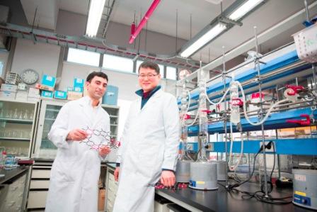
Whereas there are many difficulties in the synthesis of graphene, the team of researchers at Ulsan National Institute of Science and Technology (UNIST) and Pohang University of Science and Technology in South Korea synthesized nitrogenated 2D crystals using a simple chemical reaction in liquid phase without using a template. Conventional methods for the formation of 2D crystals require the use of such a template. The researchers verified the structure of the nitrogenated crystal by atomic-resolution scanning tunnelling microscopy imaging and confirmed its semiconducting nature by testing it with a field effect transistor. The unique geometric and electronic structure of the nitrogenated crystals make it potentially suitable for use in electronics, sensors and catalysis. Its successful synthesis using a simple technique may open a new chapter in the cost-effective generation of other 2D materials.
“We believe that the results presented in this work provide not only compelling advance in materials science and technology, but also exciting potential for a wide range of practical applications from wet-chemistry to device applications,” says Professor Jong-Beom Baek, professor of the School of Energy and Chemical Engineering at UNIST. “Thus, the material would attract immediate attention from a broad range of disciplines, due to its potential scientific and technological impacts,” he says.
The findings of the study appeared in Nature Communications on March 6, 2015. (Nat. Commun. 6:6486 doi: 10.1038/ncomms7486 (2015))


