Cellphone users rely on their phone cameras to capture virtually every aspect of their lives. Far too often, however, they end up with photos that are a sub-par reproduction of reality.
While operator error sometimes comes into play, the camera’s digital image sensor is the most likely culprit. A flat, silicon surface, it just can’t process images captured by a curved camera lens as well as the similarly curved image sensor — otherwise known as the retina — in a human eye.

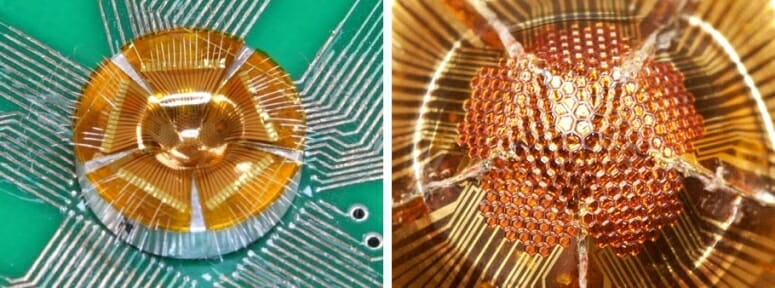
In an advance that could lead to cameras with features such as infinite depth of field, wider view angle, low aberrations, and vastly increased pixel density, flexible optoelectronics pioneer Zhenqiang (Jack) Ma has devised a method for making curved digital image sensors in shapes that mimic the convex features of an insect’s compound eye and a mammal’s concave “pinhole” eye.
Along with his students and collaborators, Ma, the Lynn H. Matthias and Vilas Distinguished Achievement Professor of Electrical and Computer Engineering at the University of Wisconsin–Madison, described the technique in a study published today (Nov. 24, 2017) in the journal Nature Communications.
Curved image sensors do exist. Yet even though they outperform their flat counterparts, they haven’t made it into the mainstream — in part, because of the challenges inherent in a manufacturing method that involves pressing a flat, rigid piece of silicon into a hemispherical shape without wrinkling or breaking it or otherwise degrading its quality.
Ma’s technique was inspired by traditional Japanese origami, the art of paper folding.
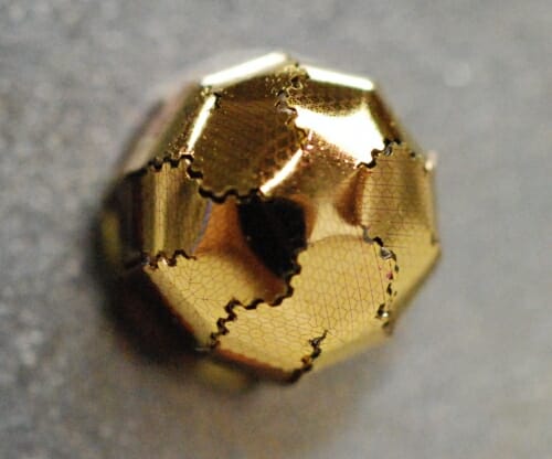
To create the curved photodetector, Ma and his students formed pixels by mapping repeating geometric shapes — somewhat like a soccer ball — onto a thin, flat flexible sheet of silicon called a nanomembrane, which sits on a flexible substrate. Then, they used a laser to cut away some of those pixels so the remaining silicon formed perfect, gapless seams when they placed it atop a dome shape (for a convex detector) or into a bowl shape (for a concave detector).

“We can first divide it into a hexagon and pentagon structure, and each of those can be further divided,” says Ma. “You can forever divide them, in theory, so that means the pixels can be really, really dense, and there are no empty areas. This is really scalable, and we can bend it into whatever shape we want.”
Pixel density is a boon for photographers, as a camera’s ability to take high-resolution photos is determined, in megapixels, by the amount of information its sensor can capture.
The researchers’ current prototype is approximately 7 millimeters — roughly a quarter-inch — in diameter. That’s still a bit bulky for your cellphone, but Ma says he can make the sensor even smaller.
“This membrane is a very big advance in imaging,” he says.
Other authors on the paper include Kan Zhang, Yei Hwan Jung, Solomon Mikael, Jung-Hun Seo, Munho Kim, Hongyi Mi, Han Zhou, Zhenyang Xia, Weidong Zhou and Shaoqin Gong. They have patented the advance through the Wisconsin Alumni Research Foundation.


