Tohoku University’s Center for Innovative Integrated Electronic Systems, in collaboration with the University of Cambridge has published a study that uses hexagonal boron nitride as a tunnel barrier for ferromagnetic tunnel junctions.
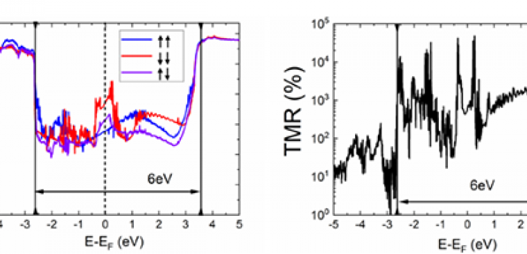
Tohoku University’s Center for Innovative Integrated Electronic Systems (CIES) has been working collaboratively with the University of Cambridge under the core-to-core project (PL: Prof. Endoh). JSPS has announced an analysis using two-dimensional (2D) materials (hexagonal boron nitride; h-BN) as a tunnel barrier for ferromagnetic tunnel junctions (MTJ), which can expect a tunnel magnetoresistance (TMR) ratio of up to 1,000% and interfacial perpendicular magnetic anisotropy (IPMA).
The state-of-the-art MTJs in an MRAM device comprising three layers of CoFeB/MgO/ CoFeB and it has been practically used with the key functions of Δ1 coherent tunneling and interfacial perpendicular magnetic anisotropy (IPMA). Δ1 coherent tunneling increases the MTJ’s high output and spin transfer torque-switching efficiency.
IPMA contributes to the reliability of data retention for over 10 years. Professors John Robertson and Hiroshi Naganuma explains, “We calculated the perpendicular conduction and IPMA of 2D materials by considering the future integration of 2D materials and MTJs.” A future is envisioned in which in-plane/perpendicular conduction is composed of 2D materials by integrating transistors and MTJs with the high in-plane mobility of 2D materials and the electric field effect.
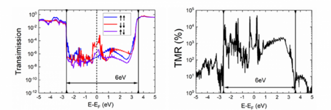
The international collaboration team discovered the relative positional relationship between the atoms of Co and N enhances the IPMA due to the hybridization of orbital at the interface between the 2D material (h-BN) and the ferromagnetic metal (Co, Fe). We predicted a tunnel magnetoresitance (TMR) ratio of up to 1,000% appears in a ferromagnetic tunnel junction (MTJ) using h-BN as a tunnel barrier.
“Weak and flexible” chemical bonding by van der Waals force gives freedom to design in ferromagnetic tunnel junctions. As a result, expectations for hybrid integrated circuits that combine in-plane/perpendicular conduction by utilizing the high in-plane mobility of 2D materials and tunnel conduction in the direction perpendicular to the plane.
The results were published online in August as the editor’s choice in the Applied Physics Review.
In above figure shows the transmission function and overall calculated TMR ratio for five layers of h-BN and Co. It has been found that the TMR ratio is highest at a relatively long interatomic distance assuming that the top layer of Co and the h-BN layer are physically adsorbed, and a TMR ratio up to 1,000% can be theoretically obtained.
The paper also reports on the relationship between various atomic positions and the TMR ratio, and it was found that the relative atomic arrangement relationship has a large effect on the TMR ratio as was found with the Graphene case. Therefore, to obtain a high TMR ratio, it is necessary to control the atomic positional relationship using advanced crystal growth technology.
The team calculated three types of atomic positional relationships when setting the interfacial of Co and h-BN and investigated the IPMA. Figure 2 shows the energy phase diagram when Co is placed directly on N. It was found that IPMA is induced by orbital hybridization of h-BN and Co. In this orbital hybridization, the orbital between the dz2 orbital of the Co layer and the N pz orbital in h-BN are mixed, and the empty downspin Co dz2 state shifts upward (and the N pz state shifts downward).
As shown, it stabilizes the filled N pz state of the surface layer and induces IPMA. From the calculation in Figure 2, the interaction when N is placed directly above Co shifts the empty PDOS downspin band of the Co layer upward by +1 eV, resulting in hybridization. This means that there is a mutual downward shift of the occupying bond states of N pz, thus increasing the occupancy bond and providing IPMA.
In summary, it was found that h-BN induces IPMA with a high TMR ratio, and the weak chemical coupling based on van der Waals force gives us freedom in the selection of ferromagnetic materials, which is advantageous in design in MTJ stacking.
Furthermore, the research of transistors using high in-plane mobility is being developed in the 2D materials, and the clarification of its usefulness in tunneling conductance through this research is a significant achievement that will contribute to the development of integrated 2D devices in the future.


