A simple technique for mass producing ultrathin, high-quality molybdenum trioxide nanosheets could lead to next-generation electronic and optoelectronic devices.
Molybdenum trioxide (MoO3) has potential as an important two-dimensional (2D) material, but its bulk manufacture has lagged behind that of others in its class. Now, researchers at A*STAR have developed a simple method for mass producing ultrathin, high-quality MoO3 nanosheets. [1]
Following the discovery of graphene, other 2D materials such as transition metal di-chalcogenides, began to attract considerable attention. In particular, MoO3 emerged as an important 2D semiconducting material because of its remarkable electronic and optical properties that hold promise for a range of new applications in electronics, optoelectronics and electrochromics.
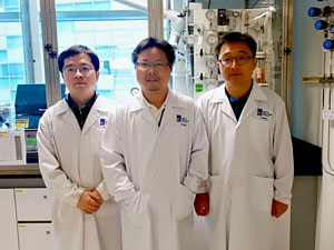
Liu Hongfei and colleagues from the A*STAR Institute of Materials Research and Engineering and Institute of High Performance Computing have sought to develop a simple technique for mass producing large, high-quality nanosheets of MoO3 that are flexible and transparent.
“Atomically thin nanosheets of molybdenum trioxide have novel properties that can be utilized in a range of electronic applications,” says Liu. “But to produce good quality nanosheets, the parent crystal must be of very high purity.”
By first using a technique called thermal vapor transport, the researchers evaporated MoO3 powder in a tube-furnace at 1,000 degrees Celsius. Then, by reducing the number of nucleation sites, they could better match the thermodynamic crystallization of MoO3 to produce high-quality crystals at 600 degrees Celsius without the need for a specific substrate.
“In general, crystal growth at elevated temperatures is affected by the substrate,” explains Liu. “However, in the absence of an intentional substrate we could better control the crystal growth, allowing us to grow molybdenum trioxide crystals of high purity and quality.”
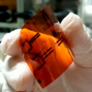
After cooling the crystals to room temperature, the researchers used mechanical and aqueous exfoliation to produce submicron-thick belts of MoO3 crystals. Once they subjected the belts to sonication and centrifugation, they were able to produce large, high-quality MoO3 nanosheets.
The work has provided new insights into the interlayer electronic interactions of 2D MoO3 nanosheets. The crystal growth and exfoliation techniques developed by the team could also be helpful in manipulating the band gap — and therefore the optoelectronic properties — of 2D materials by forming 2D heterojunctions.
“We are now attempting to fabricate 2D MoO3 nanosheets with larger areas, as well as exploring their potential use in other devices, such as gas sensors,” says Liu.
The A*STAR-affiliated researchers contributing to this research are from the Institute of Materials Research and Engineering and Institute of High Performance Computing. For more information about the team’s research, please visit the Electronic Materials (ELE) webpage.


