Flexible and foldable high-performance barrier or encapsulation technology had long represented a technology challenge.
The industry spent a decade and a half optimizing the approaches and the processes to achieve large-area production-grade results.
The development however has not ended. Indeed, the commercial journey towards flexible and foldable devices is only just beginning. As such, the development of flexible barrier technologies still has far to travel.
The development however has not ended. Indeed, the commercial journey towards flexible and foldable devices is only just beginning. As such, the development of flexible barrier technologies still has far to travel.
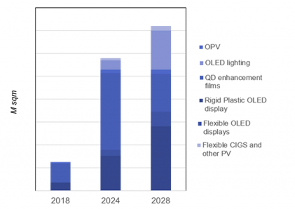
In this article, we provide a brief overview of the evolution of the technology to its current status and consider some of the latest technology trends that seek to replace current incumbent techniques. This overview is drawn from our report “Barrier Films and Thin Film Encapsulation for Flexible and/or Organic Electronics 2019-2029”. This report provides a detailed study of this technology space, examining the needs, analysing existing and emerging technology options, evaluating application requirements and market potentials, assessing different players worldwide, and offering market forecasts segmented by application (rigid OLED, flexible OLED, plastic rigid OLED, OLED lighting, OPV, CIGS, QDs, etc) and barrier technology (TFE, MLB, single-layer ALD, thin-glass, etc).
Roll-to-roll barrier film production
The performance requirements for flexible barrier layers were, and are, difficult to meet. The barrier requirements are often expressed in terms of WVTR (water vapor transition rate) and vary from 1e-3 to 1e-6 g/sqm/day, depending on the application. This is many orders of magnitude beyond the ability of plastic substrates to meet. As such, layered and highly-engineered barriers were required.
Furthermore, the encapsulation layer must (a) exhibit low stress to prevent cracking and delamination during repeated bending, (b) offer high optical transparency, and (c) benefit from high deposition rates over large areas to drive down TACT. Ideally, the overall structure can also be made extremely thin to enable a development roadmap towards and beyond a 1mm bending radius and can be manufactured at high yield with few deposition machines and steps. Clearly, simultaneously satisfying all these requirements has been, and remains, a technological and an engineering challenge.
As such, over the years, numerous technologies have been proposed and developed to meet this WVTR. In general, thus far, a multi-layer structure has mainly been utilized. This structure consists of alternative dyes of organic and inorganic materials. The alternative structure decouples the position of the defects, creating a tortuous path. The generally much thicker organic layer serves to planarize the surface, covering larger particulate and plugging pinholes, whilst also acting as a stress release structure to promote flexibility.
At first many focused on roll-to-roll (R2R) production of multilayer barrier films. The idea was that high web speeds and wide web widths together with an intrinsically low bill of materials would enable the driving down of the cost of barriers, thus helping unlock the potential of many applications including organic photovoltaics (OPVs), OLED lighting, and flexible OLED displays. This approach however has thus far proved too difficult. Most implementations were on narrow web machines and achieved reported champion results only at very low web speeds.
Furthermore, the entire machine engineering had to be adapted to minimize electrostatic build-up, to achieve uniform heat distribution, and, most challengingly, to avoid or at least minimize contact with the coated side of the film during film rolling or wind-up. Many innovative approaches were proposed and developed. However, few crossed the chasm towards large-web format. In addition, the need for a highly-impermeable and flexible adhesive was an additional disadvantage of this approach. Critically, the main variable in the cost of production here was yield which also affects web speed (due to film quality). Given the lack of substantial existing markets, the producers struggled to find enough production learning opportunities to assess and to improve their yield. As such, real validation was not demonstrated.
In displays, the film type has so far given way to conformal direct thin film encapsulation (TFE). Despite this, the developments on film type are still ongoing. There is engagement with other emerging markets which require barrier films. There are also improvements inface-seal adhesive technology (e.g., hot-melt type with embedded particles or others that can dramatically relax WVTR of the barrier itself with potentially significant beneficial consequences) and production processes including fully-solution processed techniques.
Even in terms of display markets, firms are taking the longer-view, hoping that they can (a) deliver a cost advantage (e.g., high web speeds, lowering yield requirements, etc) in the longer term for next-gen mother glass (substrate) sizes, and/or (b) offer a more accessible technology to new display producers who do not have the in-house know-how and/or the expensive equipment set to produce in-line TFE. To learn more, please see our report “Barrier Films and Thin Film Encapsulation for Flexible and/or Organic Electronics 2019-2029”, this report will provide a comprehensive view of the technologies, applications, players, and existing and future markets.

The incumbent: thin film encapsulation (TFE)
This approach is also based on a multi-layer structure principle. Indeed, it is essentially an evolution of the original Vitex approach. This approach is now commercialized on Gen6 production lines. In its current state, the inorganic SiNx layer is PECVD deposited at low temperature and the organic layer is inkjet printed and then cured. In previous generations, PVD and through-mask evaporation were used for the inorganic and organic layers, respectively. These transitions in production processes, as well as extensive optimization,have dramatically reduced layer numbers from 11 to 3, thus reducing equipment count, production steps, and overall TACT, whilst boosting flexibility and transparency. This is no easy feat especially as high yields must be maintained over a Gen6 mother substrate. This is critical because defects are expensive as they will waste the entire device including the TFT and OLED structure. The recent news about a Korean display maker having to suspend production on one of its Gen6 lines due to TFE quality further demonstrate the scale of this challenge.
Future trends of TFE technology
There are trends to further evolve TFE technology too. Atomic layer deposition (ALD) is proposed as a superior deposition technology over PECVD. ALD does produce high-quality films at a lower thinness although the low thinness can limit extrinsic performance despite high intrinsic barrier values. However, temporal ALD is ill-suited to large-area deposition given its low deposition rates. Spatial ALD does improve the productivity however it is still an immature technology that has been mainly demonstrated on narrow-web films or on small-sized silicon wafers. Companies had attempted to also implement s-ALD on large-sized glass substrate however none were yet production-qualified. The developments on ALD will however continue, especially as PECVD replacement, since a key driver is to continually narrow down the TFE structure without performance compromise.
In another development, an all-PECVD process is being developed with a potential for a single-chamber deposition. Here, the structure is composed of an inorganic layer (e.g., SiNx), a buffer adhesion layer (e.g., SiONx) an organic layer, and a stress reduction layer (e.g.,SiONx). The organic layer is fluorinated plasma-polymerized hexamethyldisiloxane (pp-HMDSO:F) which is plasma deposited through a mask. Significant knowhow exists in processing the pp-HMDSO:F without causing spraying, premature reactions, and other technical issues. There are however issues to resolve such as: cleaning the mask, boosting material utilization, fine-tuning the chemistry, etc. Note that the role of the stress reduction layer is to have a layer with a built-in tensile strength to counteract the compressive stress of the underlying layer, thus helping reliability and optical transparency. The approach has been demonstrated using Gen-4.5 tools, achieving promising results including 200k cycle test around a 2.5R radius. Furthermore, this approach reduces the thickness of the organic layer to 1-2um, a significant improvement in the thickness levels achieved by the incumbent inkjet-printed organics.
In another development, a special solution processed layer is being developed. This layer can be solution cast to replace the vacuum deposited inorganic layer, thus boosting process time and reducing CapEx investments to make the technology more accessible to a wider range of producers. The layer can be cured at temperatures around 120C (2min) and will require an argon plasma treatment step to improve film quality. This film can withstand high temperatures, thus making it a good option for the bottom barrier on backplane technologies such as LTPS. It can also be used as the top barrier. Here, it could be solution coated on a planarizing organic layer atop the OLED structure. This method has been demonstrated on Gen2.5 substrates, achieving 5E-6 g/sqm/day and passing 200k bending test around a 3mm radius. This technique has already been licensed to two or more firms, seeking to leverage the solution processability to produce low-cost high-performance barrier films.
Many have already reported single-layer barrier results using ALD or PECVD. In using the latter, the chemistry of the inorganic layer can be graded to improve performance. Indeed, promising results exceeding the required WVTR are often reported. However, it is doubtfulwhether extrinsic WVTR can also be maintained over large areas and the bendability tests passed without the additional organic layer. This is an ongoing area of research. Many are also working on incremental but important improvements such as enhancing organic-to-inorganic adhesion, improving yield, shaving small amounts off the thickness, and so on. In general, with time, the TFE stack will be further simplified and thinned, the TACT time and production step shortened, and yield improved even over larger mother substrate sizes.


